

Now we are living in the world of technology. The electronics is the back bone of all the new technologies. The electronics field is an exponentially growing field. Are you think about that? What is the main tuning point in the electronic field. Every body say that it is the discovery of transistors, most precisely the discovery of INTEGRATED CIRCUIT. We call it as IC, in short form. Basically what is an IC, Is it a discrete component like capacitor, transistor, resistor, etc... Are you think about it. I think about it in my childhood. For solving this question I broken an IC chip and observe it. But nothing seems inside it, only a small square shaped reflecting silicon chip. Then after some years I found that, that small part is the IC chip, all other black part is only the packaging. So I wondered about it. I search much more about it and find that, it is not a discrete component it is a circuit (as the name indicates), it contain the basic components like resistors, capacitors, transistors, etc... So here I make a discrete chip by using the basic components. I use the famous 555 timer chip. I make its original circuit using basic components in a PCB. So first we discuss something about the 555 and then start to make our on discrete 555. OK.


555 Timer Chip
The worlds most popular IC is the 555. It used in all the equipment from the toy to the airplanes. I started my IC electronic carrier with this 555 IC. It is a very useful IC. It is used as oscillator, modulator, electronic switch, PWM generator, mono stable and bi-stable multi vibrator, etc... It the internet there is a huge amount of 555 circuits. It is an 8 pin IC. It is in DIP or in the smd package. It contain 23 transistors, 2 diodes and 16 resistors. In the following section explain more about it.
555 Pinout
It has 8 legs, 4 in each sides.
Pin 1 :- Ground
It is the negative supply or the ground voltage pin. Here the negative of the supply connected.
Pin 2 :- Trigger
It is the trigger pin. It is one of the input of the 555 IC. It is connected to the comparactor and it compare the trigger voltage with 1/3 of the Vcc voltage.
Pin3 :- Output
It is thge output pin. It produce both positive and negative voltages at the output. It capable of delivering 200mA of current.
Pin 4 :- Reset
It is the reset pin. It is used to reset the internal flip-flop. It is active positive. So it is commonly connected to Vcc.
Pin 5 :- Control voltage
It is the control voltage pin. It is used to change the comparactor reference voltage of 2/3 Vcc to any other value. Commonly it is used for modulation purpose. Otherwise it is connected to ground via a .01uF capacitor to stabilize the control voltage.
Pin 6 :- Threshold
It is the threshold pin. It is connected to one of the comparactor which compare it with the 2/3 of the Vcc voltage.
Pin 7 :- Discharge
It is the discharge pin. Basically it is an output pin. It produce only negative voltages. It is commonly used for astable operation.
Pin 8 :- Vcc
It is the Vcc pin. It is used to power up the IC. It is ranges from 2V to 15V.
555 block diagram

The 555 block diagram represent the internal structure of 555. It contain a voltage divider, 2 comparators, SR flip-flop, output driver. The voltage divider produce 1/3 Vcc, 2/3 Vcc voltages. These are connected to non-inverting and inverting inputs of each comparators respectively. The other 2 inputs are used for trigger and threshold input. Its output is connected to the inputs of SR flip-flop. Its output is connected to the driver and discharge pin for oscillator circuit purpose. SR flip-flop produce output of previous state, 0, 1 for 00,01,10 SR input respectively. The 11 input combination is invalid. Here it is not used. The input sequences are controlled by user via the comparator. The output produce logic one and logic zero voltages. It deliver maximum of 200 mA, so no need of external buffers for connecting to relay. The whole circuit is work from 3 V to 15 V. The reset pin reset the flip-flop when it is low. The upper voltage divider node is connectrd to external control voltage pin to change the comparator voltage for modulation purposes.
Comparactor working
 The above figure indicate the symbol of a comparactor. It is basically an op-amp configured at infinity gain. For an op-amp, the gain is infinity when there is no feedback. The output of comparactor is positive or the negative only (only 2 states). The output is obtained by comparing the two inputs.
When voltage at + input < voltage at - input then output is negative voltage.
When voltage at + input > voltage at ₋ input then output is positive voltage.
SR Flip-Flop working
The SR flip-flop symbol and its truth table is given in the figure. Flip-flop is a device used to store a data value. It has 2 inputs. Its value determine the output value. It is given in the figure.

Inside 555 chip
 The 555 is not a discrete component. It is a circuit by using transistors , resistors, etc... in a single silicon chip. The IC chip making is a special technique that contain several complex steps. It is complex because the size of the chip is very small. The 555 ic is a circuit by using transistors, diodes and resistors in a single chip. The wafer image( die image) is given above. It is the complete 555 circuit. It contain 23 transistors, 2 diodes, 16 resistors. By using reverse engineering technique we are find the exact component level circuit. Here the component level circuit is given. It is a BJT realization circuit. It is also available in CMOS version. In the die image the large three identical structures is the output driver transistors and discharge transistor. These are large because it handle more current than others. In the BJT circuit image the colour boxes represent the corresponding block names. It is given in the block diagram above mentioned.

Chip Making
Here explain how to make the chip. The actual chip is about 1.5 m.m x 1.5 m.m in size. Our discrete chip is about 37 m.m x 28 m.m in dimension. About 1 : 460 in area. It is a huge difference. This is a small chip so the discrete 555 size is comfort for us. But compare this scaling with a microprocessor which contain millions of transistor, It is a non-imaginable one. My dream is to create a discrete microprocessor or a micro controller. I try it later. Here I made the full chip by using through hole components because it is easy to handle. The whole circuit created in a pref-board because it enhance your circuit solving ability. The PCB making using software's decrease your circuit solving abilities. So I prefer pref board. Here I complete the whole circuit into a small piece of PCB. But it is too difficult. It need more experiences. So you choose yours favorable size. Try to minimize to its limit.
Our Circuit

In the above image shows the circuit we are going to create. Here the diodes are replaced by transistors by shorting its base and emitter. It is because in the original manufacturing process it done like this. So the two diodes are replaced by the transistors. Here in the output section and discharge section I use S8050 transistor because it deliver much more current. All other transistors are general purpose transistors. Here I use different transistors because I am take it from old circuit boards. In my opinion you follow this manner. This is a good way to experience the de-soldering and soldering. It reduce the cost and it is save our planet by reusing the waste. You use any general purpose transistors. But NPN and PNP not changeable. But take care about the pin configuration of transistors which are you chosen. Pin configuration is different for different transistors it is based on the package of the transistor. OK. Only keep the NPN and PNP in its position and use any general purpose transistors instead of my transistors. But remember one thing, in a block using of same transistor is better because of the identical characteristics, for example in the comparator section use one type and in flip-flop side use another type. I use the transistors in this manner. The transistor pin-out is given above and the datasheets are given below.
Full circuit making procedures is given in my instructables. Please visit it. Link is given below.
Components Needed
Pref-board - 1
Connecting wires
PCB connector male
 Transistors PNP
BC557 - 4
A1015 - 6
C9015 - 2
C9012 - 1
Transistor NPN
C945 - 10
SS8050 - 3
Resistors
 100E - 1
220 E - 1
820 E - 1
1 K - 1
3.9 K - 1
4.7 K - 7
6.8 K - 1
10 K - 1
15 K - 1
100 K - 2
Circuit Debugging
For circuit debugging, the test points are given in the figure. The procedures given below.
- First check all connection with respect to the circuit diagram
- Visually check for any unwanted shorts in the PCB
- Then double check all the connections using multi meter which operating at continuity position
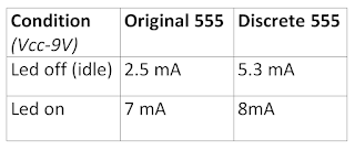
- Then apply a 9V to the 555 PCB through an ammeter and if ammeter show less than 10 mA then test pass otherwise it indicates any short in the circuit or presence of failed transistors
- After completing the above steps successfully check the 3 test point voltages using multi meter when the PCB connected as in the circuit above. The test points also given in above
- Vary the potentiometer and compare the obtained results with the standard results given below ( my supply voltage is 8V)
TP 1 -- 0.7V when Vin > pin 6 cutoff voltage (2/3 Vcc, here it is 5.2V)
TP 1 -- 0.0V when Vin < pin 6 cutoff voltage (2/3 Vcc, here it is 5.2V)
TP 2 -- 0.6V when Vin< pin 2 cutoff voltage (2/3 Vcc, here it is 2.6V)
TP 2 -- 0.2V when Vin > pin 2 cutoff voltage (2/3 Vcc, here it is 2.6V)
TP 2 -- 0.2V when Vin > pin 2 cutoff voltage (2/3 Vcc, here it is 2.6V)
TP 3 -- 1.44V when Vin > pin 2,6 cutoff voltage (2/3 Vcc, here it is 5.2V)
TP 3 -- 0.0V when Vin < pin 2,6 cutoff voltage (2/3 Vcc, here it is 2.6V)
TP 3 -- 0.0V when Vin < pin 2,6 cutoff voltage (2/3 Vcc, here it is 2.6V)
- If test point 1 fails, then it is the problem of threshold comparactor
- If test point 2 is fails, then it is the problem of trigger comparactor
- If test point 3 is fails, then it is the problem of the flip-flop
- After all success testing, connect an led to output and vary the potentiometer (from 0% to 100%) and if led is on and off then the output stage is working otherwise output stage has a problem
- If all the steps complete successfully then follow next steps otherwise check the defected block, the main causes for failing are failed connection, shorts in the soldering, failed transistor, wrong transistor polarity, etc...
- Observations
- The 555 chip frequency is little bit higher than the original 555. I believed that it is due to the comparactor cutoff voltage difference between the original 555 and our 555 chip. I guess that this difference make the frequency difference. But our circuit work very well. You try to test it with other 555 circuits.
- For checking the working status of reset pin connect it to the ground. If the led blinking stops, then it indicate the working condition.
- More observation is given below.

- Full making procedures is given in my instructables. Link given below.
- https://www.instructables.com/id/Working-MEGA-555/
thanks for these great articles dear your blogger is very Good i like your blogger tanks again and check it
ReplyDeleteadobe photoshop 7.0 for pc free download
.
Top 25 SEO tips and tricks to follow in 2020
.
Facebokk Photo verification Bypass 2020 Latest trick
.
How to root any android Device without pc easy way
.
jazz free internet code 2020
.
how to unlock pta blocked phone
.
telenor free internet code 2020
Great efforts. You deserve applause. Thanks.
ReplyDeleteAmazing article
ReplyDeleteTank capacitor manufacturer in India
Thanks for sharing your useful information, Chip Tuning Melbourne | Diesel Tuning Melbourne.
ReplyDeleteThanks For sharing this Superb article.I use this Article to show my assignment in college.it is useful For me Great Work. 2cl3512h
ReplyDelete
ReplyDeleteGood information.
----------------------------------------
I work in visit Stabilit America
Building a discrete 555 timer using transistors provides hands-on insight into circuit design, much like piecing together the warmth and structure of a quilted sherpa jacket . Just as each component of the jacket contributes to its comfort and style, every transistor in the circuit works together, achieving reliable timing functionality.
ReplyDeleteA brilliantly crafted piece that expertly combines deep technical knowledge with practical, real-world relevance. With outstanding clarity, rich detail, and highly actionable insights, it stands as a must-read resource for professionals dedicated to advancing their expertise in lighting design and modern innovation.
ReplyDeleteIntegrated Circuits (ICs)
A standout, expertly written article that merges technical precision with real-world relevance, offering powerful insights into modern lighting technology.
ReplyDeleteEnrgtech Electrical Components
Sharp thinking for professionals developing the next generation of solutions.
ReplyDeleteEnrgtech Electrical Solutions
Custom Woven Patches Maker No Minimum Personalized Patch Solutions Design woven patches with your logo, artwork, or branding. Our no-minimum ordering option makes it easy to create samples, prototypes, or small production runs.
ReplyDeleteOrder Custom Woven Patches Online Sharp Detail and Professional Quality Upload your artwork and order custom woven patches online. Available with sew-on, iron-on, Velcro, and adhesive backing options for versatile applications.
ReplyDeleteWhat Materials Are Used in Custom Iron On Patches for Quality and Durability? The materials used in custom iron on patches play a crucial role in appearance, durability, and performance. Common options include twill, cotton, denim, polyester, leather, and specialty fabrics. Understanding the strengths of each material helps ensure the perfect balance of style, functionality, and longevity for your custom patch project.
ReplyDelete