 |
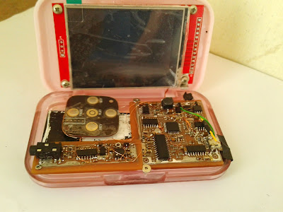
| Finished pocket oscilloscope |
It is basically a small scaled digital oscilloscope. It is capable of displaying all type of waveform like sine, triangular, square, etc. It's bandwidth is above 1 MHz and input impedance is about 600K. The device is mainly using the ATmega328 micro-controller as the heart and is assisted by a high performance ADC (TLC5510) which is capable of taking up-to 20 mega samples per second and thus increasing the span of bandwidth which can be analyzed by our device. In addition to that, in-order to make the device portable Li-ion battery is used , which will be suitable to be fitted into a confined space. Intelligent circuits have been designed to properly charge and to assist in intelligent discharge of the battery, which increase the battery life and also the contribute to boost up the reliability of the device. The screen used here is a 2.8" TFT color display (320x240).
The initiative behind this project is a similar project in the given web link, http://bobdavis321.blogspot.com/2015/06/arduino-5msps-oscilloscope-revisited.html
For my home made oscilloscope video, watch the given video,
The initiative behind this project is a similar project in the given web link, http://bobdavis321.blogspot.com/2015/06/arduino-5msps-oscilloscope-revisited.html
For my home made oscilloscope video, watch the given video,
Block Diagram
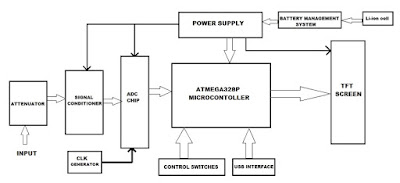
The block diagram of the entire product design is shown below. This figure makes the basic construction idea of the product clear and could help to get a basic understanding of its
internal working.Overall, the design consist of a front end, which includes an attenuator accompanied by a signal conditioner. Then follows the ADC part which samples the analog input. The next part is the heart of the design, the controller of the arduino (ATMEGA 328), which processes the sampled data. Next is the TFT screen which displays the processed output from the controller. In addition to that a power supply unit consisting of adequate circuitry to provide specific power to different components in the device is also employed.
Attenuator
The attenuator block is the main part of the front end design of the scope. The attenuator section consists of mainly two parts. They are :
Frequency compensated potential divider circuit :
Basically a frequency compensated potential divider is a 2 port RC network providing a fixed voltage division ratio over a wide frequency range. In this arrangement capacitors are added parallel to each resistors. It reduces the parasitic capacitance of the resistors which is highly active at high frequencies.That is, at low frequencies the resistors act as the voltage divider but at high frequencies capacitors act as the voltage divider circuit. Here the compensated potential divider divides the input voltage in the ratios 1:1, 2:1, 5:1 and 10:1.
Analog multiplexer:
It is used to select required input attenuated signal. It is used to replace the manual rotary input selection switch to a digitally controlled switch. The multiplexer IC used in the design is the IC HEF4052B, which is a Dual 4-channel analog multiplexer/demultiplexer. It is a wide-band 4 to 1 analog multiplexer. It is controlled by a 2 bit binary input. The multiplexer have a series of channel from 2Y0 to 2Y3 , which is selected to a common channel 2Y COM, similarly a series of channel from 1Y0 to 1Y3 which is selected to a common channel 1Y COM. S0 and S1 are the 2 bit control switching part. Only one set of channel is utilized in our design and the unused set of channel is shorted together and is grounded to avoid unwanted interference from those ports.
This section provides a high input impedance and low output impedance in the circuit by using an op-amp. This section avoids the loading effect which can be caused by feeding the signal to the ADC chip. The operational amplifier used in the conditioner design is NJM4565. The signal after attenuation is received by the positive input terminal 1 of the op amp. This signal is buffered without inverting and the boosted signal is to the ADC chip. A negative feedback to the inverting terminal 1 will set the gain to unity. The second op amp channel is used to provide a shift to the signal, for which it is connected to a preset, which can be adjusted to produce a particular DC level. This produced DC level is fed along with the boosted output, so as to produce the desired shift before sampling. This section also provides a protection against high voltage input, because the supply voltage for the op amp is only 3 volts, so if in case an input of greater volts is applied then the op amp could only provide a maximum of 3 volts, thus keeping the associating circuits safe and sound. Above all there is an additional protection circuit provide at the delivering end which is constituted by a switching diode package.
Analog to Digital Converter
ATmega328 has the provision to directly accept analog input and process it. But the sampling rate of Atmega328 is very low. Lower sampling rate will result in a very unpleasant output signal in the display, thus reducing the efficiency of the scope. As a solution to this problem, an additional ADC chip having very high sampling rate is used. The chip used here is TLC5510. The chip is capable of sampling the signal at a rate of 10MSPS to 15 MSPS. The full scale voltage input is restricted to 2V.
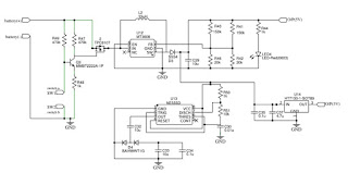
This is definitely one of the most delicate and important section for the entire design. This section produce different voltages for each parts. All the necessary voltages are generated from the Lithium-ion cell. It makes the device portable. Mainly the power supply section consist of three parts a Boost converter, 555 charge pump and a 3V regulator. Boost converter provides a stable 5 volt supply for micro-controller and ADC. The boost converter is realized using the DC-DC converter IC MT3608. I previously published a BLOG named "DIY Tiny 5V / 2A Boost Converter". Which is about this boost converter. For knowing more details, please visit it. The 555 charge pump circuit provides the negative power supply for signal conditioner. Using 555 as a charge pump is a cheap and easy solution for doubling tripling or inverting the supply voltage. Charge pump can be used in a non-synchronous rectifier when in low dropout mode to cause a high output ripple with a light load. The 3 volt regulator is used to generate voltage for display. The 3.3 volt is generated by the IC HT7130 which is a low drop out linear regulator.
The front end of the circuit is constituted by a switching mechanism as shown above. The device is equipped with this type of mechanism to switch it ON and OFF, instead of conventional toggle or push switches. This is added to facilitate an auto switch ON and OFF, while opening or closing the device respectively. The circuit diagram which depicts the entire constituents of the power supply unit. When the switch point A and B are closed, then the base of the transistor is grounded, driving the transistor to OFF state and the MOSFET gate is getting a positive voltage, which drives it to conduction mode, driving the entire device to power ON state. When the switch is open, the transistor is on and the MOSFET is having a gate voltage of zero, making it open and driving the device into OFF mode.
Battery Management System
The power house of the entire device is the lithium ion cell (3.7V). The cell is capable of providing necessary power but it is very dangerous to handle. The reason for that is lithium-ion batteries may even explode if the handling is careless and improper.The design includes a protection circuit to cancel the after effect of short circuit incidents and also an over voltage protection. This system also includes an intelligent battery charging system to keep battery in good condition. I published a BLOG named "Intelligent Li-ion Cell Management System". In that blog I explain the circuit details and working very well. For more information please visit it.
USB Interface
USB interface is provided a provision for firmware updation. It helps to connect the processor with the computer, which enables the user for proper updation and even slight program modifications. This section consist of only a single chip with minimum external components. The CH340 is a serial to USB chip used to implement the USB interfacing facility. It is a USB bus converter chip and it can realize USB convert to serial interface. It has full speed USB device interface conform to USB specification version 2.0, only needs crystal and capacitance external. It emulates standard serial interface.
Display
The display used is a 2.8 inch TFT (Thin Film Transistor) display. It has a 240 x 320 pixel resolution. It is a full color LCD display. This module is built in with IL19341V IC. The output pins from the micro-controller is connected through a resistor divider network to the TFT display. This is to ensure that only voltage less than 3.3 volts is reaching the display pins, since the power supply voltage of the display is 3.3 volts and anything above that at the pins will destroy the display module.
ADC Clock Circuit
The clock circuit is the most important circuit for any digital devices. It provide the timing sequence for the efficient working of the circuit. Here the clock circuit is made by using a combination of NOT gate IC and a crystal. Here we made a 16 MHz clock. The unused input pins are all grounded to avoid noise interference. I explained about it in my previous BLOG named"". For more details please visit it.
Full Circuit Diagram
The given two images show the full circuit diagram. The circuit is dived into main circuit and frond end circuit because I plan to make 2 PCB separately for each. I explained each parts separately in above. I draw the circuit diagram by using online EasyEDA application. |
| Main PCB circuit diagram |
 |
| Frond end PCB circuit diagarm |
PCB Layout
The given two images show the PCB layouts of the 2 PCBs. It also designed in the EasyEDA platform. Here I use SMD components for the full PCB design. It is because I interested in SMD components more than the through hole components. I use some of the components from old PCBs by using the desoldering techniques. It will reduce the project cost. The components resistors, capacitors, etc, are easily obtained from old PCBS. |
| Main PCB layout |
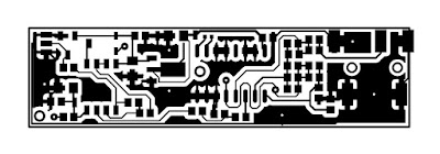 |
| Frond-end PCB layout |
If you are not familiar with SMD desoldering. Please watch my SMD desoldering tutorial videos. It is given below. It is definitely helpful for you. Please watch and support me.
SMD soldering and Wire Connections
For soldering the components I use a good tweezers and a SMD rework station. The given images shows the completed PCBs. The PCB and display are interconnected by using the small enameled copper wire.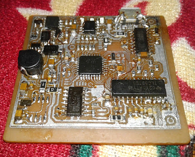 |
| Main PCB (After soldering) |
 |
| Frond-end PCB (After soldering) |
If you are not familiar with SMD soldering, the given SMD soldering video definitely helpful for you. Please watch and support me.
PROGRAM FLOW
- Import all necessary packages
- Define output and input pins
- Setup the necessary variables
- Wait for an input positive or negative going trigger
- Quickly collect and store the data with no delay
- Display the collected data
- Check the status of push button switches
- Change the variable values accordance with input data through push switches
- Update the text on the right side
- End of program



Please help me to build this project
ReplyDeletehello.
ReplyDeletepcb document??
This comment has been removed by the author.
ReplyDeleteopen source?
ReplyDeleteHow to contact you want to discuss something related to this project plz reply asap
ReplyDeleteNeed the program for tested
ReplyDeleteGood information.
ReplyDelete-------------------------------------------------
I work in fiberglass roofing panels
"Very great post.Thanks for sharing this post.
ReplyDeleteLooking for reliable DC motors? Tomson Electronics offers a premium selection perfect for various industrial and hobbyist applications. Known for their simplicity, durability, and cost-effectiveness, Motors are ideal for precise control and continuous rotation. Visit Tomson Electronics for all your motor and electronic component needs!"